The Art of Electronics: The X Chapters - by Horowitz Hill
Wow did you hear about that new sequel coming out? No, no, not The Matrix 4 – it's The Art of Electronics - X Chapters! More delicious, practical electronic advice from the masters, Paul Horowitz and Winfield Hill.
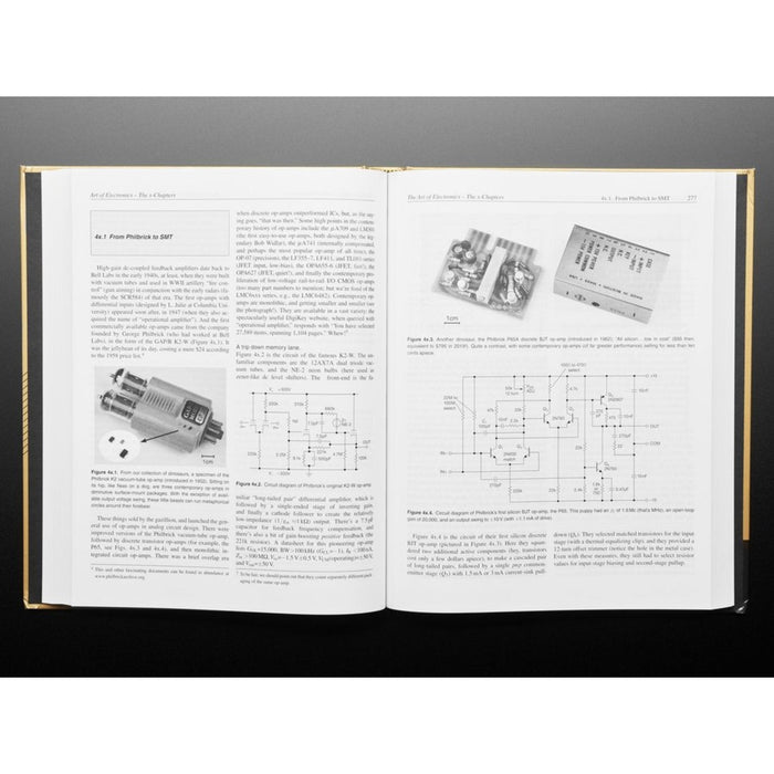
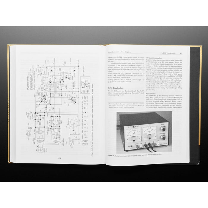
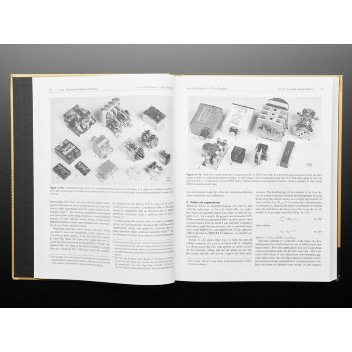
The Art of Electronics: The X Chapters expands on topics introduced in the best-selling third edition of The Art of Electronics, completing the broad discussions begun in the latter.
In addition to covering more advanced materials relevant to its companion, The X Chapters also includes extensive treatment of many topics in electronics that are particularly novel, important, or just exotic and intriguing.
This enticing spread of electronics wisdom and expertise will be an invaluable addition to the library of any maker, student, researcher, or practitioner with even a passing interest in the design and analysis of electronic circuits and instruments. You'll find techniques and circuits that are available nowhere else!
Clocks in at a whopping 500+ pages with 45 tables - so prepare yourself for a very long and informative book club!
Contents
- List of Tables
- Preface
-
ONE: Real-World Passive Components
- 1x.1 Wire and Connectors
- 1x.1.1 Wire gauge: resistance, heating, and current-carrying capacity
- 1x.1.2 Stranding, insulation, and tinning
- 1x.1.3 Printed circuit wiring
- 1x.1.4 PCB traces
- Resistance and current-carrying capacity; Capacitance and inductance; Transmission-line impedance and attenuation
- Transmission-line impedance and attenuation
- 1x.1.5 Cable configurations
- 1x.1.6 Inductance and skin effect
- 1x.1.7 Capacitive and magnetic coupling
- 1x.1.8 Mitigation of coupled signals
- 1x.1.9 Shielded enclosures
- 1x.1.10 Connectors
- 1x.1.11 Connectors for RF and high-speed signals
- 1x.1.12 High-density connectors
- 1x.1.13 Connector miscellany
- 1x.2 Resistors
- 1x.2.1 Temperature coefficient
- 1x.2.2 Self-capacitance and self-inductance
- 1x.2.3 Nonlinearity (voltage coefficient)
- 1x.2.4 Excess noise
- 1x.2.5 Current-sense resistors and Kelvin connection
- 1x.2.6 Power-handling capability and transient power
- Do-it-yourself testing; Overload to failure
- 1x.2.7 Resistor dividers
- 1x.2.8 “Digital” Resistors
- The digipot zoo; Digipot cautions; Wrapup
- 1x.3 Capacitors
- 1x.3.1 Temperature coefficient
- 1x.3.2 ESR
- 1x.3.3 ESL
- 1x.3.4 Dissipation factor
- 1x.3.5 Voltage coefficient of capacitance
- 1x.3.6 AC voltage coefficient
- 1x.3.7 Aging
- 1x.3.8 Frequency dependence of capacitance
- 1x.3.9 Electromechanical self-resonance and microphonics
- 1x.3.10 Dielectric absorption
- 1x.3.11 Capacitor choices for typical applications
- Bypass and decoupling; Oscillators, filters, and timing; High frequency; Energy storage; AC line filtering; High voltage
- 1x.3.12 Capacitor miscellany
- 1x.4 Inductors
- 1x.4.1 The basics
- 1x.4.2 Air-core inductors
- Solenoid – approximate; Solenoid – exact; Toroid; Loop
- 1x.4.3 Magnetic-core inductors
- Ferromagnetic materials; Ferrite-core solenoid; Ferrite-core toroid; Gapped core; Noise and spike suppression
- 1x.4.4 Inductors and transformers for power converters
- 1x.4.5 Why build it, when you can buy it?
- 1x.4.6 Inductor examples
- Radiofrequency “chokes” and bias-T’s
- 1x.5 Poles and Zeros, and the “s-Plane”
- 1x.6 Mechanical Switches and Relays
- 1x.6.1 Why use mechanical switches or relays?
- 1x.6.2 So what’s the problem?
- Relay and switch contact life; Contact protection; Relay coil suppression; Improving relay switching speed
- 1x.6.3 Other switch and relay parameters
- Switches: Function, actuator, bushing, terminals; Relays: Moving-armature, reed, and solid-state
- 1x.7 Diodes
- 1x.7.1 Diode characteristics
- The family tree; Reverse (leakage) current; Forward voltage drop; Dynamic impedance; Peak current; Reverse capacitance; Zener capacitance
- 1x.7.2 Stored charge and reverse recovery
- Reverse recovery test circuit; Dependence on reverse and forward currents; Dependence on diode size; Schottky and fast-recovery diodes; Soft-recovery diodes; Step-recovery diodes; A farout step-recovery application: Larkin’s 40-amp kilovolt pulser; What about forward recovery?
- 1x.7.3 The tunnel diode
- Current versus voltage: Region of negative resistance; Measuring the tunnel diode characteristic curve; Tunnel diode trigger circuit
- 1x.7.1 Diode characteristics
- 1x.8 Miscellaneous Circuits with Capacitors and Inductors
- 1x.8.1 Improved leading-edge detector
- 1x.8.2 Capacitance multipliers
- 1x.1 Wire and Connectors
-
TWO: Advanced BJT Topics
- 2x.1 What’s the Actual Leakage Current of BJTs and JFETs?
- 2x.2 Current-Source Problems and Fixes
- 2x.2.1 Improving current-source performance
- 2x.2.2 Current mirrors: multiple outputs and current ratios
- 2x.2.3 Widlar logarithmic current mirror
- 2x.2.4 Current source from Widlar mirror
- 2x.3 The Cascode Configuration
- 2x.4 BJT Amplifier Distortion: a SPICE Exploration
- 2x.4.1 Grounded-emitter amplifier
- 2x.4.2 Getting the model right
- 2x.4.3 Exploring the linearity
- Input–output transfer function; Gain versus input
- 2x.4.4 Degenerated common-emitter amplifier
- 2x.4.5 Differential amplifier
- Estimating the distortion
- 2x.46 Differential amplifier with emitter degeneration
- 2x.4.7 Sziklai-connected differential amplifier
- 2x.4.8 Sziklai-connected differential amplifier with current source
- 2x.4.9 Sziklai-connected differential amplifier with cascode
- 2x.4.10 Caprio’s quad differential amplifier, with cascode
- 2x.4.11 Caprio’s quad with folded cascode – I
- 2x.4.12 Caprio’s quad with folded cascode – II
- 2x.4.13 Measured distortion
- 2x.4.14 Wrapup: amplifier modeling with SPICE
- 2x.5 Early Effect and Early Voltage
- 2x.5.1 Measuring Early effect
- 2x.5.2 Some Early effect formulas
- 2x.5.3 Consequences of Early effect: Output resistance
- Maximum single-stage voltage gain; Current-source output impedance
- 2x.6 The Sziklai Configuration
- 2x.6.1 Two-transistor “standard” Sziklai
- 2x.6.2 Three-transistor “enhanced” Sziklai
- 2x.6.3 Push–pull output stage: a Sziklai application
- 2x.7 Bipolarity Current Mirrors
- 2x.7.1 A simple high-speed bipolarity current source
- Reducing input current; Operating at higher voltages
- 2x.7.2 Precision bipolarity current source with folded cascode
- 2x.7.1 A simple high-speed bipolarity current source
- 2x.8 The Emitter-Input Differential Amplifier
- 2x.8.1 An application: High-current, high-ratio current mirror
- 2x.8.2 Improving the emitter-input differential amplifier
- 2x.9 Transistor Beta versus Collector Current
- 2x.10 Parasitic Oscillations in the Emitter Follower
- 2x.11 BJT Bandwidth and fT
- 2x.11.1 Transistor amplifiers at high frequencies: first look
- Reducing the effect of load capacitance
- 2x.11.2 High-frequency amplifiers: the ac model
- ac model; Effects of collector voltage and current on transistor capacitances; Low- and highcurrent regions; SPICE parameters; Comparing SPICE models with measured fT; Wideband micropower BJTs; Collector–base time constant and maximum oscillation frequency
- 2x.11.3 A high-frequency calculation example
- 2x.11.1 Transistor amplifiers at high frequencies: first look
- 2x.12 Two-terminal Negative Resistance Circuit
- 2x.13 If It Quacks Like an Inducktor . . .
- 2x.14 ‘‘Designs by the Masters”: ±20 V, 5 ns, 50 Ω Amplifier
- 2x.14.1 Output stage block diagram
- 2x.14.2 Output stage: the full enchilada
- 2x.14.3 Output stage: some fine points
- 2x.14.4 Epilogue: 120 V, 5 A, dc-10 MHz Laboratory Amplifier
- Circuit details; Output protection; Transistor choices
-
THREE: Advanced FET Topics
- 3x.1 A Guided Tour of JFETs
- 3x.1.1 Gate current, IGSS and IG
- 3x.2 A Closer Look at JFET Transconductance
- 3x.2.1 Dependence of gm on ID
- 3x.2.2 Dependence of gm on VDS
- 3x.2.3 Performance of the transconductance enhancer
- 3x.2.4 Transconductance in the JFET source follower
- 3x.3 Measuring JFET Transconductance
- 3x.4 A Closer Look at JFET Output Impedance
- 3x.4.1 A JFET’s gos-limited gain, Gmax
- 3x.4.2 Source degeneration: another way to mitigate the gos effect
- 3x.4.3 Dependence of gos on drain current density
- 3x.4.4 Dependence of gos and Gmax on VDS
- 3x.4.5 A parting shot: gos – sometimes it matters, sometimes it doesn’t
- 3x.4.6 Example: A low-noise open-loop differential amplifier
- 3x.5 MOSFETs as Linear Transistors
- 3x.5.1 Output characteristics and transfer function
- Datasheet curves; Measured data
- 3x.5.2 Linear operation: hotspot SOA limitation
- 3x.5.3 Exploring the subthreshold region
- MOSFETs at low drain voltage; MOSFETs at high drain voltage
- 3x.5.4 Exploring a high-voltage
- MOSFET
- IXTP1N120 transfer characteristics; IXTP1N120 transconductance 3x.5.5 SPICE models for power
- MOSFETs in the subthreshold region
- 3x.5.6 Typical SPICE model for a power MOSFET
- Equivalent circuit; Model capacitances; Other models
- 3x.5.7 An unusual low-voltage MOSFET
- 3x.5.1 Output characteristics and transfer function
- 3x.6 Floating High-Voltage Current Sources
- 3x.6.1 Raising output impedance with a cascode
- 3x.6.2 Reducing power dissipation
- 3x.6.3 Small-signal output impedance
- 3x.6.4 Low-cost predictable current source
- 3x.6.5 Current sources for higher voltages
- A simple scheme; Distributed series string; Some applications: HV amplifier; HV probe; Highvoltage current sources: 250 µA; High-voltage current sources: 2 mA; Current sources in highvoltage amplifiers; High-voltage current sources: 5 mA and more; Perfect high-voltage current source
- 3x.7 Bandwidth of the Cascode; BJT versus FET
- 3x.7.1 The common-gate/ common-base amplifier
- 3x.7.2 Cascode as common-gate/ common-base amplifier
- 3x.7.3 Estimating cascode bandwidth
- 3x.7.4 What about MOSFETs?
- 3x.7.5 Bandwidth of the source follower
- 3x.8 Bandwidth of the Source Follower with a Capacitive Load
- 3x.8.1 Follower with resistive signal source
- 3x.8.2 Follower driven with a current signal
- 3x.9 High-Voltage Probe with High Input Impedance
- 3x.9.1 Compensated-offset MOSFET follower
- 3x.9.2 Bootstrapped op-amp follower
- 3x.10 CMOS Linear Amplifiers
- 3x.11 MOSFETs Through the Ages
- 3x.11.1 A MOSFET Saga: the First 30 Years
- 3x.11.2 The next 15 years
- Logic-level gates; Packages; Pchannel MOSFETs; High-voltage parts; Capacitances
- 3x.11.3 Four kinds of power MOSFETs
- Comparison of capacitances; Energy: what does all this capacitance stuff mean? Conclusion
- 3x.12 Measuring MOSFET Gate Charge
- 3x.12.1 The gate charge curve depends on load current
- 3x.12.2 Gate charge curves at constant load current
- 3x.12.3 The gate charge curve depends also on drain voltage
- 3x.12.4 Gate charge test circuit
- 3x.12.5 The Miller plateau
- 3x.13 Pulse Energy in Power MOSFETs
- 3x.13.1 Limited only by maximum junction temperature
- Controlled Conduction; Avalanche Mode
- 3x.13.2 Alternative graphs
- 3x.13.1 Limited only by maximum junction temperature
- 3x.14 MOSFET Gate Drivers
- 3x.15 High-Voltage Pulsers
- 3x.15.1 Two-switch +600 V pulser
- 3x.15.2 Two-switch +500 V 20 A fast pulser
- 3x.15.3 Two-switch reversible kilovolt pulser
- 3x.15.4 Output monitor
- 3x.15.5 Three-switch bipolarity kilovolt pulser
- 3x.16 MOSFET ON-Resistance versus Temperature
- 3x.17 Thyristors, IGBTs, and Wide-bandgap MOSFETs
- 3x.17.1 Insulated-gate bipolar transistor (IGBT)
- 3x.17.2 Thyristors
- 3x.17.3 Silicon carbide and gallium nitride MOSFETs
- 3x.18 Power Transistors for Linear Amplifiers
- 3x.19 Generating Fast High-Current LED Pulses
- 3x.19.1 10 ns pulser
- 3x.19.2 High-power pulser
- Wiring; Gate voltage; Power dissipation
- 3x.19.3 Integrated LED Drivers
- 3x.20 Precision 1.5 kV 1 µs Ramp
- 3x.21 Fast Shutoff of High-Energy Magnetic Field
- 3x.21.1 Helmholtz coils, rapid field shutoff
- 3x.21.2 High voltage, high current switches
- 3x.22 Precision Charge-dispensing Piezo Positioner
- 3x.22.1 Fast MOSFET pulsed charge dispenser
- 3x.22.2 Analog charge dispenser
- 3x.22.3 Small-step pulsed charge dispenser
- 3x.1 A Guided Tour of JFETs
-
FOUR: Advanced Topics in Operational Amplifiers
- 4x.1 From Philbrick to SMT
- 4x.2 Feedback Stability and Phase Margins
- 4x.2.1 Sliding f 2: phase margin and circuit performance
- 4x.2.2 What about amplifiers with GCL>1?
- 4x.2.3 Applying Bode plots to amplifier design
- 4x.2.4 Afterword: High-speed op-amps
- SPICEing the 3-pole op-amp
- 4x.3 Transresistance Amplifiers
- 4x.3.1 Stability problem
- 4x.3.2 Stability solution
- 4x.3.3 An example: PIN diode amplifier
- Gaining speed; “Pedal to the metal”; Sub-picofarad capacitors
- 4x.3.4 A complete photodiode amplifier design
- 4x.3.5 Gain-switching
- 4x.3.6 Some loose ends
- 4x.3.7 Designs by the masters: A wide-range linear transimpedance amplifier
- 4x.3.8 A “starlight-to-sunlight” linear photometer
- 4x.3.9 Autoranging wideband transimpedance amplifier
- 4x.3.10 Multiple-range cascode-bootstrap wideband TIA
- 4x.4 Unity-Gain Buffers
- 4x.4.1 Stability of the composite amplifier
- 4x.4.2 Some more applications
- 4x.4.3 Some cautions
- 4x.5 High-Speed Op-amps I: Voltage Feedback
- 4x.5.1 Voltage feedback and current feedback
- Some confusing terms
- 4x.5.2 Overview of the table
- 4x.5.3 Scatterplots: Seeking trends
- 4x.5.1 Voltage feedback and current feedback
- 4x.6 High-speed Op-amps II: Current Feedback
- 4x.6.1 Properties of CFBs
- Closed-loop bandwidth; Slew rate and output current; The feedback network and stability; Input current and precision
- 4x.6.2 Care and feeding of CFBs
- 4x.6.3 “Hybrid” VFB+CFB op-amps
- 4x.6.4 When to use CFBs
- 4x.6.5 Mathematical postscript: bandwidth and gain in CFBs
- 4x.6.6 Remarks on the table
- 4x.6.1 Properties of CFBs
- 4x.7 Power Supply Rejection Ratio
- 4x.8 Capacitive-Feedback Transimpedance Amplifiers
- 4x.8.1 Capacitive-feedback TIA for gigabit optical receivers
- 4x.9 Slew Rate: A Detailed Look
- 4x.9.1 Increasing slew rate
- 4x.9.2 Case study: high-voltage pulse generator
- 4x.10 Bias-Current Cancellation
- 4x.10.1 The best of both worlds?
- 4x.10.2 Bias cancellation: the circuits
- Simplest: Mirroring the base current of a cascode twin; Better: Bootstrapping the cascode bias; Another way: replicating the emitter current
- 4x.10.3 Bias cancellation: how well does it work?
- 4x.11 Rail-to-Rail Op-amps
- 4x.11.1 Rail-to-rail inputs
- 4x.11.2 Rail-to-rail outputs
- 4x.11.3 Output near ground: when “RRO” isn’t
- 4x.11.4 Offsetting the negative supply terminal 338
- 4x.11.5 Designs by the masters: the Monticelli output stage
- 4x.12 Slewing and Settling
- 4x.12.1 Dependence on fT
- Slew-rate enhanced op-amps
- 4x.12.2 A caution: ’scope overdrive artifacts
- 4x.12.1 Dependence on fT
- 4x.13 Resistorless Op-amp Gain Stage
- 4x.14 Silicon Photomultipliers
- 4x.14.1 SiPM characteristics
- 4x.14.2 SiPM construction
- 4x.14.3 SiPM characteristics, electronics, and waveforms
- 4x.15 External Current Limiting
- 4x.16 Designs by the Masters: Bulletproof Input Protection
- 4x.17 Canceling Base-Current Error in the Current Source
- 4x.18 Analog “Function” Circuits
- 4x.18.1 The Lorenz attractor
- 4x.18.2 Summing amplifiers
- Non-inverting Adder; Adder– subtractor
- 4x.19 Normalizing Transimpedance Amplifier
- 4x.20 Logarithmic Amplifier
- 4x.20.1 Temperature compensation of gain
- 4x.21 A Circuit Cure for Diode Leakage
- 4x.22 Capacitive Loads: Another View
- 4x.22.1 Frequency of oscillation
- 4x.22.2 So, how about a few equations?
- 4x.23 Precision High-Voltage Amplifier
- 4x.23.1 Overview
- 4x.23.2 High-voltage output stage
- 4x.23.3 Front-end amplifier stage
- 4x.23.4 Feedback stability
- 4x.23.5 Circuit capacitances and capacitive loads
- No load, no feedback capacitance; Add feedback capacitance; Add load capacitance; Output series resistor; SPICE analysis
- 4x.23.6 Output slew rate
- 4x.23.7 Measured performance
- 4x.23.8 Variations: unipolarity, higher voltages, greater speed
- MOSFET transistor choices
- 4x.23.9 Faster HV amplifier: 1MHz and 1200V
- Transistor choices; Circuit changes
- 4x.24 High-Voltage Bipolarity Current Source
- 4x.24.1 Performance issues
- 4x.25 Ripple Reduction in PWM
- 4x.26 Nodal Loop Analysis: MOSFET Current Source
- 4x.26.1 Example: MOSFET current source
- Nodal model; KCL equations; Node equations; Results
- 4x.26.2 Example: fast 2.5 A pulsed current
- 4x.26.1 Example: MOSFET current source
-
NINE: Advanced Topics in Power Control
- 9x.1 Reverse Polarity Protection
- 9x.2 Lithium-Ion Single-Cell Power Subsystem
- 9x.2.1 Charger features
- 9x.2.2 Monitor and Protect
- 9x.2.3 Output voltage regulator
- 9x.2.4 Multiple cells: a “battery”
- 9x.3 Low-Voltage Boost Converters
- 9x.4 Foldback Current Limiting
- 9x.5 PWM for DC Motors
- 9x.5.1 The myth: PWM as secret sauce
- An experiment; Toy trains and sewing machines; Another experiment
- 9x.5.2 Wrapup: PWM versus dc for motor drive
- 9x.5.3 Afterword: DC motor model
- Series resistance: Op-amp analogy
- 9x.5.1 The myth: PWM as secret sauce
- 9x.6 Transformer + Rectifier + Capacitor = Giant Spikes!
- 9x.6.1 The effect
- 9x.6.2 Calculations and cures
- 9x.7 Low-Voltage Clamp/Crowbar
- 9x.7.1 New clamp/crowbar
- Circuit operation; Additional details; Performance
- 9x.7.1 New clamp/crowbar
- 9x.8 High-Efficiency (“Green”) Switching Power Supplies
- 9x.9 Power Factor Correction (PFC)
- 9x.10 High-Side High-Voltage Switching
- 9x.11 High-Side Current Sensing
- 9x.11.1 Pulse generator overcurrent limit
- 9x.11.2 Current monitor for high-voltage amplifier
- Current monitor for HV bipolarity amplifier
- 9x.12 High-Voltage Discharge Circuit
- 9x.13 Beware Counterfeits (or, Don’t Bite into That Apple)
- 9x.14 Low-Noise Isolated Power
- 9x.15 Low-Current Non-isolated DC Supplies
- 9x.15.1 Simplest circuit: reactance-limited zener bias
- 9x.15.2 Improved circuit: full-wave rectifier
- 9x.15.3 Why hasn’t Silicon Valley responded?
- 9x.15.4 Case study: ceiling fan
- 9x.15.5 Inverse Marx generator
- 9x.16 Bus Converter: the “DC Transformer”
- 9x.16.1 Differences from classic switch-mode converter
- 9x.16.2 Bus converter applications
- 9x.16.3 Bus converter example
- 9x.16.4 A few comments
- 9x.17 Negative-Input Switching Converters
- 9x.17.1 Negative buck from positive boost
- 9x.17.2 Negative boost from positive buck
- 9x.18 Precision Negative Bias Supply for Silicon Photomultipliers
- 9x.19 High-Voltage Negative Regulator
- 9x.20 The Capacitance Multiplier, Revisited
- 9x.21 Precision Low-Noise Laboratory Power Supply
- 9x.21.1 Overview
- 9x.21.2 Circuit details
- 9x.21.3 Performance
- 9x.22 Lumens to Watts (Optical)
- 9x.23 Sending Power on a Beam of Light
- 9x.24 ‘‘It’s Too Hot” Redux
- 9x.24.1 The finger test
- 9x.24.2 Better thermometry
- 9x.25 Transient Voltage Protection and Transient Thermal Response
- 9x.25.1 The problem
- 9x.25.2 The solution
- 9x.25.3 TVS devices
- Gas surge arrestors; Metal oxide varistors; Zener TVSs
- 9x.25.4 MOV versus zener TVS
- 9x.25.5 “Series-mode” transient protection
- 9x.25.6 TVS circuit example
- Fast-switching magnet
- 9x.25.7 Transient test circuit
- Standard test pulses
- 9x.25.8 Transient thermal response
- Parts Index
- Subject
The The Art of Electronics: The X Chapters - by Horowitz Hill appears in the following collections:

